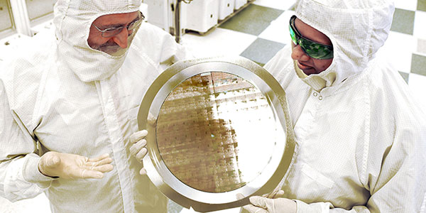
IBM Research on Thursday announced that an alliance it leads has produced the first 7nm node test chips with functioning transistors.
Big Blue’s partners are GlobalFoundries, Samsung and the State University of New York Polytechnic Institute’s Colleges of Nanoscale Science and Engineering (SUNY Poly CNSE).
The alliance sought to develop industry-first innovations, such as Silicon Germanium (SiGe) channel transistors, and Extreme Ultraviolet (EUV) lithography integration at multiple levels.
The 7nm chips are the result of the first program out of IBM’s 2014 US$3 billion investment in research — a five-year investment that aims to push the limits of chip technology to meet the needs of cloud computing and big data systems.
Using 7nm chips will allow the placement of more than 20 billion SiGe switches on fingernail-sized chips, said Mukesh Khare, vice president of IBM Semiconductor Technology Research.
“We intend to incorporate 7nm into the road maps for IBM systems in the future,” he told TechNewsWorld. “This milestone is the first step towards a silicon-based proof point with all elements demonstrated in our 300nm research facility at Albany.”
The History of SiGe Technology
IBM introduced SiGe technology into mainstream manufacturing in 1989. It currently is collaborating with AMD on program to develop SiGe stressed-silicon 65nm technology.
TSMC also offers SiGe manufacturing capacity.
Dynamite Comes in Small Packages
As companies increasingly move to the cloud and toward leveraging big data, the need for faster CPUs and more processing power grows.
However, it’s becoming increasingly difficult to attain higher clock speeds, because that generates more heat, which is becoming more difficult to dissipate. It also consumes too much power and is plagued by current leakage.
Transmission times and switching delays are a problem with higher clock speeds as well — and it’s getting increasingly expensive to make faster chips.
That has led semiconductor firms to look at packing more cores onto their processors.
The number of transistors in an integrated circuit doubles roughly every two years, according to Moore’s Law, but the semiconductor industry for some years has been concerned that it is fast reaching the upper limit of just how many transistors can be packed into an IC.
Size — or the lack of it — has become crucial.
Intel apparently expects to be able to build 5nm transistors at some point.
“The higher the density of transistors, the more cores you can put in a given space,” noted Rob Enderle, principal analyst at the Enderle Group.
“A very high-density part would be ideal for the cloud, which is why ARM and Intel are also chasing it,” he told TechNewsWorld.
Challenges IBM Will Face
The IBM alliance has to ensure that it develops technology that will let it manufacture SiGe transistor channels in high volumes, Enderle cautioned.
“This is where most of the really promising technology fails,” he pointed out. “They can get it to work in the lab, but can’t figure out how to manufacture it with high yields and low-enough costs.”
The economics of the new nodes “may become as great of a challenge as the technology,” Tirias Research Principal Analyst Jim McGregor told TechNewsWorld.
Another problem concerns EUV lithography. “Current-generation technology is so well known, so well integrated, and so cheap that the marginal cost to use something else is higher than its marginal value,” Enderle remarked.
EUV lithography “will require a top-to-bottom change in the fab — basically a brand new factory with machines that don’t exist even in prototypes yet,” he said. “There’s a high risk that by the time all of this is sorted, the traditional parts may be good enough to make the whole exercise a waste. “


